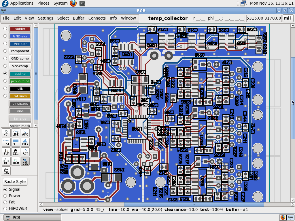
PCB is an interactive printed circuit board editor for Unix, Linux, Windows, and Mac systems. PCB includes a rats nest feature and schematic/netlist import, design rule checking, and can provide industry standard RS-274X (Gerber), NC drill, and centroid data (X-Y data) output for use in the board fabrication and assembly process, as well as photorealistic and design review images. PCB offers high end features such as an autorouter and trace optimizer which can tremendously reduce layout time. For custom requirements, PCB offers a plug-in API for inserting new functionality and using that functionality from within the GUI as well as in scripts.
PCB includes a stand-alone program (called pcb) which allows users to create, edit, and process layouts for printed circuit boards, as well as a library of footprint definitions for commonly needed elements. While originally written for the Atari, and later rewritten for Unix-like environments, it has been ported to other operating systems, such as Linux, MacOS/X, and Windows.
While PCB can be used on its own, by adding elements and traces manually, it works best in conjunction with a schematic editor such as gschem from the gEDA project, as gschem will create a netlist, make sure all the elements are correct, etc.
The file in which pcb stores its data ends in .pcb such as myboard.pcb. Additionally, pcb reads individual element footprints from files ending in .fp and netlists from files ending in .net.
There are a couple of different outputs from pcb. If you are having your boards professionally fabricated, you will want to export your board as an RS-247X (aka gerber) file. If you are fabricating your board yourself, you’ll probably want to print it. You can also save it as an encapsulated postscript or image file for use in documentation and/or web pages.
A note about typography: Throughout this document, “PCB” refers to the whole package, “pcb” refers to that specific program, and “pcb” refers to a generic printed circuit board.
Your First Board
In this chapter, we’re going to walk you through creating a few very simple boards, just to give you an idea of the way the programs work and how to do the things that are common to all project. Each board will build upon techniques learned from the previous board.
While this manual is not intended to cover the gschem program, we will be instructing you on the minimum you’ll need to know to use gschem with pcb. Please refer to the gschem documentation for further details.
The first board will be a simple LED and resistor. It will show you how to create a board, place elements, and route traces. The second board will be a simple LED blinker, which will involve creating schematics, setting up a project, and creating new symbols and footprints. The third board will be another blinker, this time with surface mount devices and four layers, which will introduce power planes, vias, and thermals.
LED Board
This first board will show you the basic operation of pcb. Each new command or operation that is introduced will be described in full the first time, but not subsequent times. Many operations can be invoked either by a menu option, like File→Quit Program to select the “Quit” option in the “File” menu, or by a keyboard shortcut, like Ctrl-Q. When we say Ctrl-Q we mean to hold the Ctrl key while pressing the Q key. When we say Shift-Q we mean to hold either Shift key while pressing the Q key.
Blinker Board
This next board will introduce some additional concepts in pcb that will help you with more complex board. It is assumed that you’ve gone through the previous board, and those concepts will not be re-explained. This board will be another single-sided board, but with additional components. We will use a schematic to describe the circuit, create some custom symbols and footprints, and learn to use the autorouter.
SMT Blinker
The third and final board in the “first board” series will teach you about multi-layer boards, vias, and SMT components. Again, we assume you’ve done the other two boards, and will not re-explain concepts taught there. We will be using the same circuit as the last board, but to make things interesting, we will be adding some constraints. The board must be as small as possible, EMI-proof, and able to handle rework. Ok, I’m making this up, but what it means is that we will be using the smallest components a hobbyist can expect to use, a four-layer board, and more vias than would otherwise be needed. We do this to give us the opportunity to learn these techniques, without spending undue time due to an overly large schematic.