KiCad is an open-source software tool for the creation of electronic schematic diagrams and PCB artwork.
- Schematic Capture
With the schematic editor you can create your design without limit; there are no paywalls to unlock features. An official library for schematic symbols and a built-in schematic symbol editor help you get started quickly with your designs.
- PCB Layout
Make professional PCB layouts with up to 32 copper layers. KiCad now has a push and shove router which is capable of routing differential pairs and interactively tuning trace lengths.
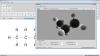
- 3D Viewer
KiCad includes a 3D viewer which you can use to inspect your design in an interactive canvas. You can rotate and pan around to inspect details that are difficult to inspect on a 2D view. Multiple rendering options allow you to modify the aesthetic appearance of the board or to hide and show features for easier inspection.
About KiCad
KiCad is an open source software suite for Electronic Design Automation (EDA). The programs handle Schematic Capture, and PCB Layout with Gerber output. The suite runs on Windows, Linux and macOS and is licensed under GNU GPL v3.
History
The first release date was in 1992 by its original author, Jean-Pierre Charras, but is now currently under development by the KiCad Developers Team.
The name of KiCad comes from the first letters of a company of Jean-Pierre Charras' friend "Ki" being combined with "Cad". But it now has no meaning other than being the name of the software suite. Mentioned by Jean-Pierre in an email.
More KiCad history, general information, and advancements can be found in Wayne’s 2015, 2016, 2017, 2018, and 2019 FOSDEM presentations.
Beneath its singular surface, KiCad incorporates an elegant ensemble of the following stand-alone software tools:
| Program name | Description | File extension |
|---|---|---|
|
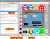
KiCad |
Project manager |
*.pro |
|
Eeschema |
Schematic editor (both schematic and component) |
*.sch, *.lib, *.net |
|
CvPcb |
Footprint selector |
*.net |
|
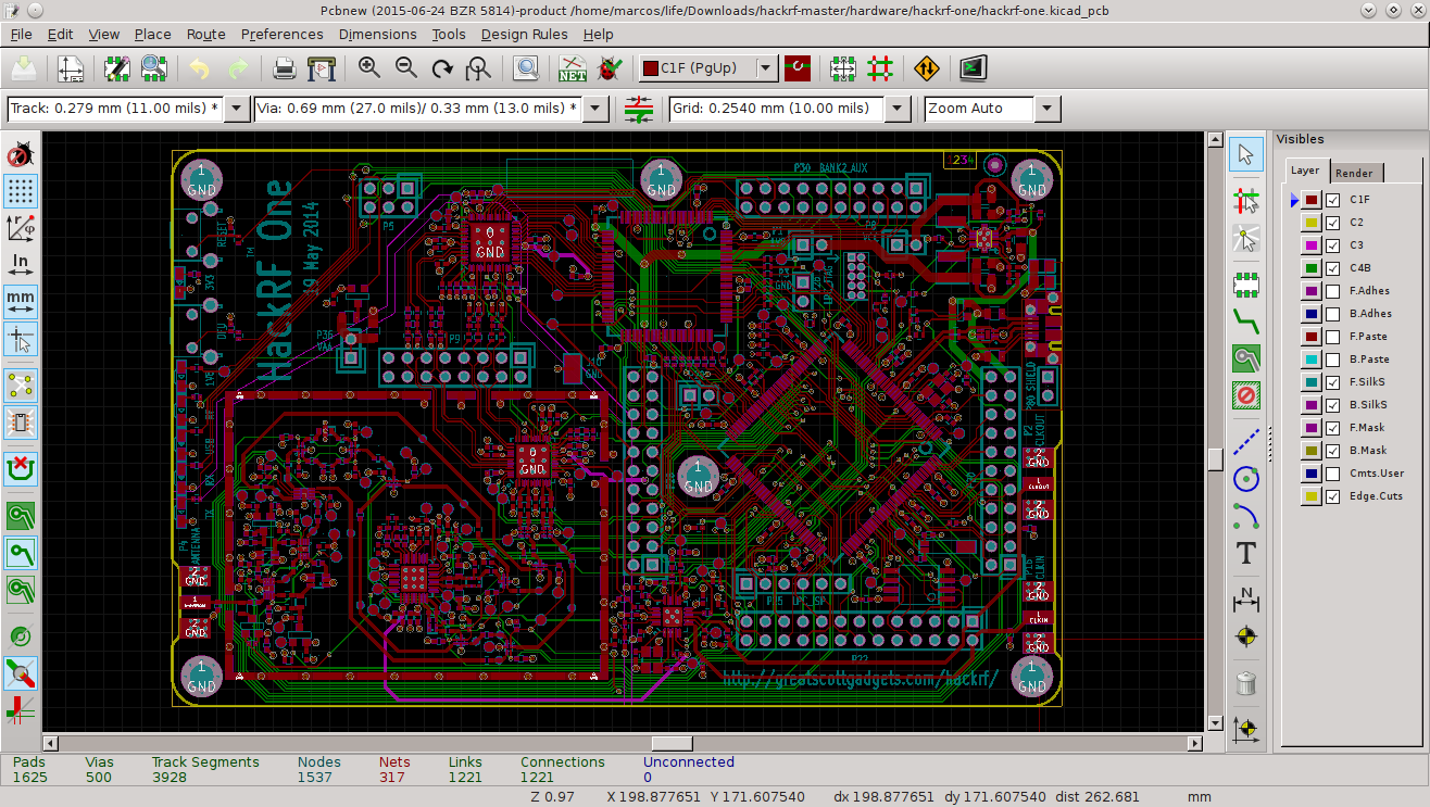
Pcbnew |
Circuit board board editor |
*.kicad_pcb |
|
GerbView |
Gerber viewer |
All the usual gerbers |
|
Bitmap2Component |
Convert bitmap images to components or footprints |
*.lib, *.kicad_mod, *.kicad_wks |
|
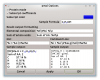
PCB Calculator |
Calculator for components, track width, electrical spacing, color codes, and more… |
None |
|
Pl Editor |
Page layout editor |
*.kicad_wks |
KiCad can be considered mature enough to be used for the successful development and maintenance of complex electronic boards.
KiCad does not present any board-size limitation and it can easily handle up to 32 copper layers, up to 14 technical layers and up to 4 auxiliary layers. KiCad can create all the files necessary for building printed boards, Gerber files for photo-plotters, drilling files, component location files and a lot more.
Being open source (GPL licensed), KiCad represents the ideal tool for projects oriented towards the creation of electronic hardware with an open-source flavour.